Logic that's fused in silicon, not loaded from memory.
Immutable. Fixed. Field-proven.
Antifuse FPGAs
One-time-programmable ViaLink® FPGAs for instant-on, mission-critical, low-power designs — trusted across three decades and more than 50 million shipped devices.
- Zero boot-up time
- Non-volatile / no bitstream to load
- 3.3 V drive / 5 V-tolerant I/O on pASIC 3 & QuickRAM
- 7 product families
- Aerospace & military heritage
- Fixed-in-structure logic for fuze & S&A safety features
Fuze & Safe-and-Arm Devices
Safety logic must remain fixed and protected from unintended alteration. Antifuse makes that inherent in the configuration technology.
- Regulatory Compliance: MIL-STD-1316F mandates that fuzing safety logic remain immutable against environmental alteration, with logic devices evaluated per JOTP-051.
- The Antifuse Advantage: QuickLogic's OTP antifuse fabric uses permanent physical interconnects rather than rewritable charge-based memory, delivering a naturally fixed-in-structure implementation.
- Streamlined Validation: Because the configuration is permanent, JOTP-051 rules requiring pre-execution integrity checks (like CRC verification) on charge-based memory do not apply to the antifuse fabric itself. Standard safety analysis and Service Safety Authority approval still apply.
Standards referenced
MIL-STD-1316F
Fuze design safety criteria. Safety-related logic must be protected from erasure, alteration, or reconfiguration by credible environments the system would otherwise survive.
JOTP-051
DoD Technical Manual for the Use of Logic Devices in Safety Features. Sets validation requirements for logic devices in safety functions, including CRC-based integrity checks when charge-based memory implements a safety feature.
Disclaimer: Acceptability of any specific implementation is determined by your program's Service Safety Authority (SSA) — this page is informational and not a compliance determination. Contact sales@quicklogic.com for datasheets and application support for fuze and S&A programs.
Availability note. Several families on this page use mature process nodes (0.18µm–0.35µm) and are best suited to sustaining or long-lifecycle programs. Before starting a new design, confirm current production status and lead times with sales@quicklogic.com.
Why antifuse
The programming element is a physical connection created at the QuickLogic Programming Center or at the engineer's desk — not in-system on a fielded board. There's no configuration SRAM to load, and no external configuration bitstream or configuration memory to extract. For legacy-system interfacing, pASIC 3 and QuickRAM provide 3.3 V output drive with 5 V-tolerant inputs.
Security by construction
Configuration is physically fused into silicon rather than loaded from external memory. There is no conventional configuration memory or external configuration bitstream to read out, substantially reducing the configuration-related attack surface associated with loadable devices.
Instant-on
Zero boot-up time makes these a fit for time-sensitive communications and munitions projects where an SRAM FPGA's load delay isn't acceptable, and where the FPGA must boot up predictably the same way every time.
Advanced clocking
Multiple global and local clock networks, with configurable clock management on supported families.
Optional embedded memory
Some families include dual-port embedded SRAM and dedicated FIFO controllers on-chip.
Low power
Antifuse configuration consumes no configuration-memory refresh power, enabling very low standby power.
Small footprint
ViaLink technology enables compact implementations for many applications.
What it means for your program
Simplified supply chain
Secure Factory Programming available with unique design part number.
Cost-effective
No separate configuration memory chip — minimizes BOM, PCB area, and total cost.
Easier certification
The absence of external configuration memory can simplify portions of system safety and security analysis.
Fast time-to-market
Prototype at your desk; production lead times are short relative to custom ASIC flows.
Better battery life
Very low standby power can extend battery life and reduce thermal load.
Field-proven
30-year history supplying more than 50 million devices across industries.
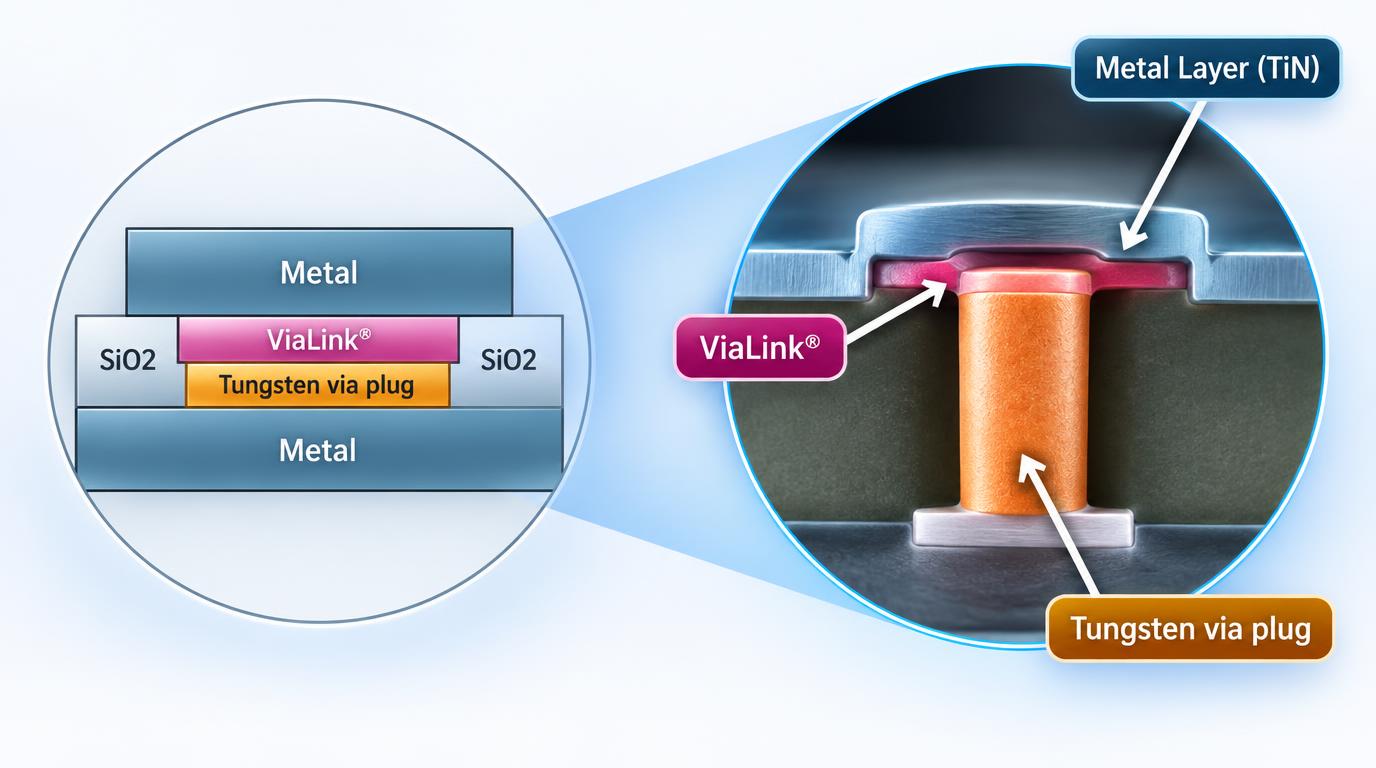
ViaLink® antifuse cross-section
How it works: ViaLink® technology
Each programmable connection point starts as a high-impedance via between two metal layers. Applying the programming voltage creates a permanent, low-resistance conductive path across that via — the inverse of a conventional fuse, and the origin of the "antifuse" name.
Because the link is a physical metal connection rather than a value stored in rewritable configuration memory, it is not erased or reloaded during normal operation. There is no conventional configuration memory or external configuration bitstream to read out, supporting the security and instant-on characteristics above.
Which family fits your design?
A quick comparison across all seven antifuse lines, from smallest footprint to highest gate count. Families and specific devices used in new designs are noted below — see each family's spec table for exact part-level guidance.
| Family | Logic cells | Process | I/O voltage support | Status | Best fit when you need… | |
|---|---|---|---|---|---|---|
| Drive | Tolerance | |||||
| pASIC 3 | 96 – 1,584 | 0.35µm, 4-layer | 3.3 V | 3.3 / 5 V | 4 of 7 Devices Recommended | The lowest-cost entry point with the widest package selection |
| QuickRAM | 160 – 1,584 | 0.35µm, 4-layer | 3.3 V | 3.3 / 5 V | Recommended | pASIC 3 array sizes plus dedicated block RAM |
| Eclipse | 960 – 4,032 | 0.25µm, 5-layer | 2.5 / 3.3 V | 2.5 / 3.3 V | 3 of 4 Devices Recommended | The Eclipse Plus array sizes without the DSP-oriented ECUs |
| Eclipse Plus | 960 – 4,032 | 0.18µm, 6-layer | 2.5 / 3.3 V | 2.5 / 3.3 V | 2 of 4 Devices Recommended | DSP-heavy signal processing, larger ECU counts, and PLLs |
| PolarPro | 512 – 7,680 | 0.18µm, 6-layer | 1.8 / 2.5 / 3.3 V | 1.8 / 2.5 / 3.3 V | Legacy | A wide range of gate counts in one low-power family, DDR-capable memory |
| PolarPro II | 864 | 0.18µm, 6-layer | 1.8 / 2.5 / 3.3 V | 1.8 / 2.5 / 3.3 V | Legacy | The smallest, narrowest-pitch package for space-constrained, low-power designs |
| Eclipse II | 128 – 1,536 | 0.18µm, 6-layer | 1.8 / 2.5 / 3.3 V | 1.8 / 2.5 / 3.3 V | Legacy | Small array sizes with optional embedded computational units (ECUs) |
I/O voltage support is family-dependent. pASIC 3 and QuickRAM provide 3.3 V drive and 5 V input tolerance; consult the applicable device datasheet for supported standards, bank configuration, and operating conditions.
“Mixed” families remain on this page in full; only the devices marked Legacy in each spec table are not recommended for new designs. Recommended and Legacy designations should reflect current QuickLogic product-management guidance; confirm status and availability with QuickLogic before design-in.
Product families
Full specifications for every antifuse line.
pASIC 3 — Lowest cost entry 4 of 7 Devices Recommended
Six base device sizes, represented by seven device variants ranging from 96 to 1,584 logic cells, available in up to seven PLCC, TQFP, PQFP, and PBGA packages. Optimized for high-speed, low-power applications and manufactured in a 0.35µm, four-layer metal CMOS process.
6 base sizes · 7 variants · 0.35µm · 4-layer metal · up to 7 package options
pASIC 3 Family Data Sheet (PDF)
| Feature | QL3004 (Legacy) | QL3004E (Legacy) | QL3006 (Legacy) | QL3012 | QL3025 | QL3040 | QL3060 |
|---|---|---|---|---|---|---|---|
| Max gates | 5,188 | 5,188 | 8,008 | 15,740 | 32,616 | 48,384 | 75,232 |
| Logic array | 8×12 | 8×12 | 10×16 | 20×16 | 28×24 | 36×28 | 44×36 |
| Logic cells | 96 | 96 | 160 | 320 | 672 | 1,008 | 1,584 |
| Max flip-flops | 178 | 178 | 322 | 438 | 876 | 1,260 | 1,900 |
| Max I/O | 74 | 74 | 74 | 110 | 196 | 244 | 308 |
| Package — PLCC 68 | 68 | 68 | 68 | – | – | – | – |
| Package — PLCC 84 | 84 | 84 | 84 | 84 | – | – | – |
| Package — TQFP 100 | 100 | 100 | 100 | 100 | 100 | – | – |
| Package — TQFP 144 | – | – | – | 144 | 144 | – | – |
| Package — PQFP 208* | – | – | – | – | 208 | 208 | 208 |
| Package — PBGA 256 | – | – | – | – | 256 | – | – |
| Package — PBGA 456 | – | – | – | – | – | 456 | 456 |
Note *: 208-pin PQFP package is in long-term obsolescence and not recommended for new designs.
QuickRAM — Block RAM on-chip 5 Devices
Five devices ranging from 160 to 1,584 logic cells, with QFN, TQFP, PQFP, and PBGA package options. Shares array sizes with the five largest pASIC 3 devices and adds block RAM. Optimized for high-speed, low-power applications and manufactured in a 0.35µm, four-layer metal CMOS process.
5 devices · 0.35µm · 4-layer metal · QFN, TQFP, PQFP & PBGA
QuickRAM Family Data Sheet (PDF)
| Feature | QL4009 | QL4016 | QL4036 | QL4058 | QL4090 |
|---|---|---|---|---|---|
| Max gates | 44,964 | 61,820 | 97,128 | 131,328 | 176,608 |
| Logic array | 16×16 | 20×16 | 28×24 | 36×28 | 44×36 |
| Logic cells | 160 | 320 | 672 | 1,008 | 1,584 |
| Max flip-flops | 242 | 438 | 876 | 1,260 | 1,900 |
| Max I/O | 74 | 110 | 196 | 244 | 308 |
| RAM modules | 8 | 10 | 14 | 18 | 22 |
| RAM bits | 9,216 | 11,520 | 16,128 | 20,736 | 25,344 |
| Max I/O — QFN 56 | – | 32 | – | – | – |
| Max I/O — TQFP 100 | 74 | 74 | – | – | – |
| Max I/O — TQFP 144 | – | 110 | 110 | – | – |
| Max I/O — PQFP 208* | – | – | 166 | 166 | 166 |
| Max I/O — PBGA 256 | – | – | 196 | – | – |
| Max I/O — PBGA 456 | – | – | – | 244 | 308 |
Note *: 208-pin PQFP package is in long-term obsolescence and not recommended for new designs.
Eclipse — 0.25µm 3 of 4 Devices Recommended
Four devices ranging from 960 to 4,032 logic cells, available in up to four PQFP, PBGA, FPBGA, and LFBGA packages. Optimized for low-power applications and manufactured in a 0.25µm, five-layer metal CMOS process.
4 devices · 0.25µm · 5-layer metal · up to 4 package options
Eclipse Family Data Sheet (PDF)
| Feature | QL6250 (Legacy) | QL6325 | QL6500 | QL6600 |
|---|---|---|---|---|
| Max gates | 248,160 | 320,640 | 488,064 | 583,008 |
| Logic array | 40×24 | 48×32 | 64×48 | 72×56 |
| Logic cells | 960 | 1,536 | 3,072 | 4,032 |
| Max flip-flops | 2,670 | 4,002 | 7,185 | 9,105 |
| Max I/O | 250 | 310 | 347 | 347 |
| RAM modules | 20 | 24 | 32 | 36 |
| RAM bits | 46,100 | 55,300 | 73,700 | 82,900 |
| Package — PQFP | 208 | 208 | – | – |
| Package — PBGA (1.27 mm) | – | – | 516 | 516 |
| Package — FPBGA (1.0 mm) | 484 | 484 | 484 | 484 |
| Package — LFBGA (0.8 mm) | 280 | 280 | 280 | 280 |
Eclipse Plus — DSP / ECU-heavy 2 of 4 Devices Recommended
The same fabric and array sizes as Eclipse, plus Embedded Computational Units (ECUs) — DSP blocks that speed up signal-processing tasks.
4 devices · up to 4 package options
Eclipse Plus Family Data Sheet (PDF)
| Feature | QL7100 (Legacy) | QL7120 | QL7160 (Legacy) | QL7180 |
|---|---|---|---|---|
| Max gates | 292,160 | 373,440 | 558,464 | 662,208 |
| Logic array | 40×24 | 48×32 | 64×48 | 72×56 |
| Logic cells | 960 | 1,536 | 3,072 | 4,032 |
| Max flip-flops | 2,670 | 3,692 | 7,185 | 9,105 |
| Max I/O | 250 | 310 | 347 | 347 |
| RAM modules | 20 | 24 | 32 | 36 |
| RAM bits | 46,100 | 55,300 | 73,700 | 82,900 |
| PLLs | 4 | 4 | 4 | 4 |
| ECUs | 10 | 12 | 16 | 18 |
| Package — PQFP (0.5 mm) | 208 | 208 | – | – |
| Package — LFBGA (0.8 mm) | 280 | 280 | 280 | 280 |
| Package — PBGA (1.0 mm) | 484 | 484 | 484 | 484 |
| Package — PBGA (1.27 mm) | – | – | 516 | 516 |
PolarPro — Widest gate range 6 Legacy Devices
Six devices ranging from 512 to 7,680 logic cells, available in up to six TFBGA, TQFP, and LBGA packages. Optimized for low-power applications across a variety of markets, manufactured in a 0.18µm, six-layer metal CMOS process.
6 devices · 0.18µm · 6-layer metal · up to 6 package options
PolarPro Family Data Sheet (PDF)
| Feature | QL1P075 | QL1P100 | QL1P200 | QL1P300 | QLP600 | QLP1000 |
|---|---|---|---|---|---|---|
| Max gates | 75,000 | 100,000 | 200,000 | 300,000 | 600,000 | 1,000,000 |
| Logic cells | 512 | 640 | 1,536 | 1,920 | 4,224 | 7,680 |
| Max I/O | 168 | 184 | 238 | 238 | 232 | 244 |
| RAM modules | 8 | 8 | 12 | 12 | 24 | 24 |
| FIFO controllers | 8 | 8 | 12 | 12 | 24 | 24 |
| RAM bits | 36,864 | 36,864 | 55,296 | 55,296 | 221,184 | 221,184 |
| CCM(s) | 2¹ | 2¹ | 2 | 2¹ | 2 | 2 |
| Package — WLCSP (0.5 mm) | 99 | – | – | – | – | – |
| Package — TFBGA (0.5 mm), 121 | – | 121 | – | – | – | – |
| Package — TFBGA (0.5 mm), 132 | 132 | 132 | 132 | 132 | – | – |
| Package — TQFP (0.5 mm) | 144 | 144 | – | – | – | – |
| Package — TFBGA (0.8 mm) | 196 | 196 | – | – | – | – |
| Package — LBGA (1.0 mm) | 256 | 256 | 256 / 324 | 256 / 324 | 324 | 324 |
¹ See datasheet for CCM configuration notes on marked devices.
PolarPro II — Smallest footprint 1 Legacy Device
A single 864 logic-cell part available in three narrow-pitch packages, optimized for low-power, small-footprint applications and manufactured in a 0.18µm, six-layer metal CMOS process.
1 device · 0.18µm · 6-layer metal · 3 packages
PolarPro II Family Data Sheet (PDF)
| Feature | QL2P150 |
|---|---|
| Max gates | 150,000 |
| Logic cells | 864 |
| RAM modules | 8 |
| FIFO controllers | 8 |
| RAM bits | 27,648 |
| CCMs | 1 |
| Max I/O — 144 VFBGA (0.4 mm pitch) | 103 |
| Max I/O — 121 TFBGA (0.5 mm pitch) | 81 |
| Max I/O — 64 WLCSP (0.4 mm pitch) | 41 |
Eclipse II — Optional ECUs 5 Legacy Devices
Five devices ranging from 128 to 1,536 logic cells, available in up to eight TFBGA, TQFP, VQFP, PQFP, PBGA, and LFBGA packages. Larger devices add Embedded Computational Units (ECUs). Optimized for smaller array-size, low-power applications and manufactured in a 0.18µm, six-layer metal CMOS process.
5 devices · 0.18µm · 6-layer metal · up to 8 package options
Eclipse II Family Data Sheet (PDF)
| Feature | QL8025 | QL8050 | QL8150 | QL8250 | QL8325 |
|---|---|---|---|---|---|
| Max gates | 47,052 | 63,840 | 188,946 | 248,160 | 320,640 |
| Logic array | 16×8 | 16×16 | 32×20 | 40×24 | 48×32 |
| Logic cells | 128 | 256 | 640 | 960 | 1,536 |
| Max flip-flops | 532 | 884 | 1,709 | 2,670 | 4,002 |
| Max I/O | 92 | 124 | 165 | 250 | 310 |
| RAM modules | 4 | 4 | 16 | 20 | 24 |
| RAM bits | 9,216 | 9,216 | 36,864 | 46,100 | 55,300 |
| PLLs | – | – | – | 4 | 4 |
| ECUs | – | – | – | 10 | 12 |
| Package — VQFP | 100 | 100 | – | – | – |
| Package — TQFP | 144 | 144 | 144 | – | – |
| Package — TFBGA (0.5 mm), 101 | – | 101 | 101 | – | – |
| Package — TFBGA (0.8 mm), 196 | 196 | 196 | 196 | – | – |
| Package — PQFP | – | – | 208 | 208 | 208 |
| Package — LFBGA (0.8 mm) | – | – | 280 | 280 | 280 |
| Package — PBGA (1.0 mm) | – | – | – | 484 | 484 |
© 2026 QuickLogic Corporation. Specifications reformatted for clarity — verify against linked datasheets before finalizing a design.